Introduction
The 2-terminal CCS formed by a pair of cascoded FETs (or depletion MOSFETs) is very popular in DIY Audio circuits. From anode loads to tail sources in an LTP stage, there are multiple applications of this simple but yet effective circuit.
I ended up designing this PCB on the back of the gyrator one as I wanted a flexible PCB which will cater for multiple design configurations as well as a variety of jFETs and MOSFETs.
I hope you will find this little board as useful as I had and please take the time to provide any feedback as is very helpful to all of us in the DIY Audio community.

PCB Features
Some key aspects of the board are:
- The PCB has been manufactured to high quality levels:
- FR4, 1.4mm thickness, ENIG finish, 2 oz. copper.
- PCB Dimensions: 57.2 mm x 33.4 mm
- M3 mounting holes spacing required (measured from each M3 hole center):
- Width: 25.3mm
- Length: 49.3mm
- 4 M3 holes
Overview
I built several boards to test the various combinations that this flexible CCS board offers:
- Top MOSFET (DN2540/IXTP08N100D) mounted close to the edge to allow the CCS to be bolted to a big heatsink. Alternative a small heatsink over the TO-220 can be used for 1-2W dissipation.
- The lower device can be multiple options depending on the target use
- High bandwidth and low noise CCS for phono stages (up to 20mA):
- 2SK170 / LSK170 (TO-92)
- BF862 (SMD)
- Alternatives to BF862 due to EOL: 2SK3557 and CPH3910
- LND150 (<1mA) – TO-92
- High bandwidth and general CCS use with jFETs:
- J310 (<60mA) – TO-92
- J112 (<5mA) – TO-92
- Protection zener for low voltage devices (jFETs)
- High-current CCS
- Gate stoppers can be either through-hole or SMD (mounted on reverse PCB side)
- Mu-follower output for low output impedance configuration
- Current measurement resistor: 1Ω or 10Ω
- Current setting arrangement:
- Fixed resistor
- Multi-turn trimpot and series resistor (optional)
- High bandwidth and low noise CCS for phono stages (up to 20mA):
Below is the diagram of the CCS board:
The circuit is very simple and just a standard cascoded MOSFET pair with depletion MOSFETs. The current of the CCS is set by either R4 or by the resistive network formed by P1 and R1 for fine adjustment. R3 is for measuring the current through the CCS. R2 and R5 are the gate stoppers needed to prevent oscillation of the MOSFETs. R6 and R7 are the SMD version of these stoppers. D1 is only needed if the lower device is a jFET which has a low VDS to protect it on start up. M1 is the MOSFET which takes all the grunt and therefore needs a heatsink depending on the current set. T1-3 doesn’t as it operates at a very low voltage across drain and source (VDS).
For circuits in which bandwidth and low noise is required, this boards provides the flexibility of using low noise jFETs and also by using a top device like the IXTP08N100D (instead of the DN25400), the lower device will operate at higher VDS therefore the leakage capacitances will be minimized. This will result in a higher overall bandwidth by improving the HF response.
Design notes
Unfortunately FETs have a wide variance on their parameters so is not easy to calculate the current setting resistor (RCCS) so we may be able to guess it or if we need precision, we need to use the trimpot. You can put a wire jumper instead of R1 and then measure the value if you want to replace P1for a fixed resistor (R4).
The CCS can be an excellent anode load in a common cathode stage. Whether as a driver or a phono stage, you can build a low noise CCS as shown below:

The now EOL BF862 can be replaced by CPH3910 or 2SK3557 which can deliver up to 20mA. The also now extinct 2SK170 can be replaced with LSK170.

Note that for very low currents you can use LND150 which can deliver up to 1.5mA. This MOSFET has to be placed on the TO-92 2SK170 position but mounted in reverse.

A popular CCS is the cascoded DN2540 pair. You can use the TO-220 version in T6 or the SMD version in T4 on the reverse side of the PCB. Depending on the package the maximum current will be either 170mA or 500mA. Watch out for the heatsink requirements on the top MOSFET (M1). Alternatively, you can use a BSP129 or BSP149 if you need up to 660mA of current capability:

For high current and precise current setting, P1 should be 100Ω or 50Ω 10 turn part:


Circuit Examples
In the following section I will provide a set of examples which are aimed to inspire the builder in the circuit design process. The board is very flexible and the few examples show only a subset of what is possible to implement.
The first example is the classic driver of a single-ended amplifier. The board is used as an anode load to the driver (V1). The CCS delivers a high impedance to V1 therefore the distortion is minimized when swinging large volts. We use the Mu output (OUT) of the board to provide a low impedance to the output valve (V2). This impedance is roughly 1/gfs where gfs is the transconductance of the lower MOSFET/jFET device at the quiescent current (Ia1):

In this case, the coupling between V1 and V2 is DC so we will need to design the stage properly to ensure that the appropriate bias is provided between the OUT and Rk1. The output stage can also be a IHT instead of the DHT. C1 provides stability to the CCS by decoupling the high impedance node. It should be mounted close to the CCS board.
The second example shown below is a slight variation of the previous design and is very popular. The coupling from V1 to V2 is via C2 and the bias arrangement of the output stage is fixed. You can use the Rod Coleman Bias Regulator or any other circuit you want to provide a stable fixed bias voltage via Rgrid. The Source Follower PCB provides the charge/discharge current of V2 input capacitance improving the slew rate response of the amplifier. This is the best sounding arrangement in my view. To simplify the power supplies, the SF board can be sourced from HV via an Rdrop/C3 stage which reduces the heat dissipated by the top MOSFET in the SF board and therefore allowing a smaller heatsink to be used. Alternatively, you could build a symmetrical bias supply (e.g. +80 and -80V) and use it to provide the negative bias voltage as well as the positive current excursion needed by the grid of V2. Remember you need at least +25-30V (50V ideally) on the top MOSFET in the SF board to operate correctly. Therefore at least a +50V supply should be used in the +B pin unless you are operating the output stage in class A2.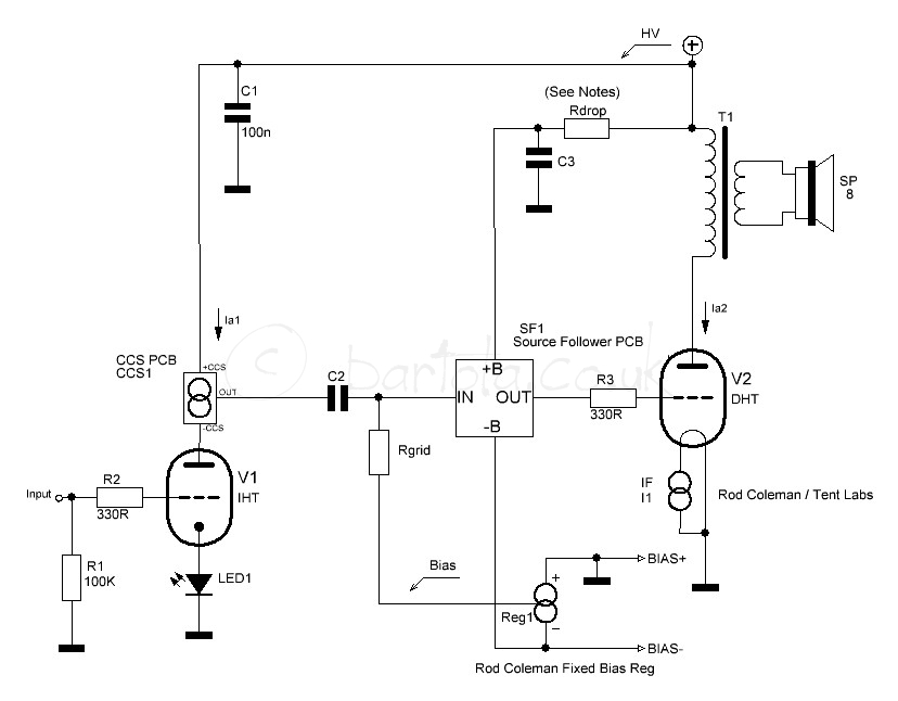
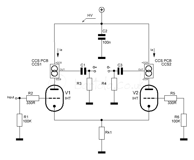
When you need a balanced signal or a driver stage for a push-pull amplifier, the LTP is a very popular circuit. In the below diagram, you can see the implementation of the LTP with 2 CCS boards as anode loads. This provides better linearity of the differential pair V1 and V2. In this case, the valves are biased with a simple resistor (RK1) but could also be either an arrangement of diodes/LEDs or another CCS. The latter should be a CCS which isn’t as stiff as the top CCSs to avoid current fighting between them (See Morgan Jones’ explanation on his book which is great).
The gas tubes (VRs) are very popular but sometimes hard to use given that we cannot load them with a big capacitor as otherwise will turn them in an oscillator. A good arrangement is shown below which is very effective if you want to have a glowing VR on the top plate (who said the VR aren’t nice?). The CCS PCB provides a stable current to set the voltage reference (V1) and isolate it from the power supply. C1 is the maximum cap you can add and R1 and C2 provides a great rejection of the raw power supply by forming a capacitance multiplier circuit with the SF PCB. The SF PCB can also have current limiter circuit built in to protect the output of the MOSFET stage.

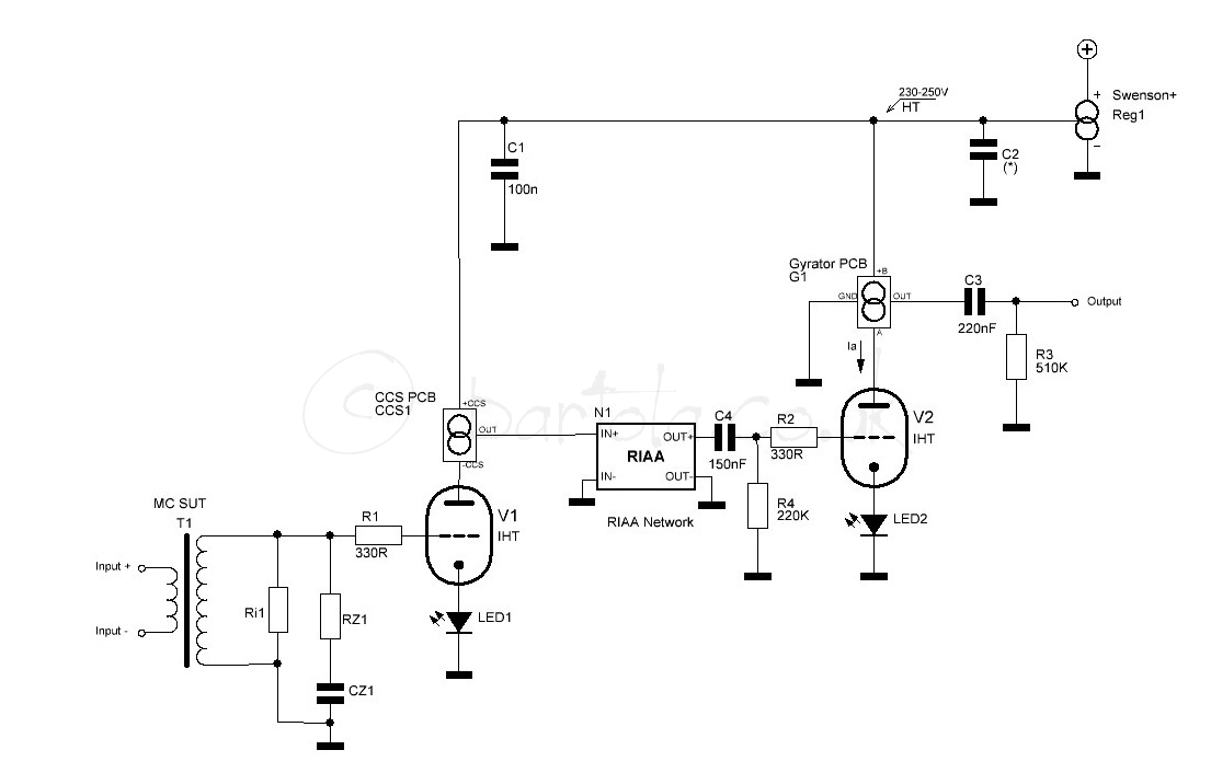
The above diagram shows a simplified RIAA phono stage. The CCS can play a great role in the first stage as anode load. By using low noise devices such as BF862 we can get the overall noise figure low. If the stage needs to be for an MC cartridge, then the MC SUT is added with its input resistor Ri1 and the Zobel network RZ1 and CZ1 which are dependent on the chosen T1.
The low output impedance of the CCS1 via the OUT pin needs to be taken into account when calculating the RIAA component values. The output stage is then any IHT or DHT with a gyrator load to ensure the driving of the cables to the amp is done effectively.
Finally, the HT is regulated and noise is kept to a minimum thanks to the Swenson+ regulator (or similar). C2 ensures stability of the circuit and should be around 10-20uF.
A nice alterantive to filament bias is shown below. This is very useful when the DHT bias is too big (e.g. 50, 300B or 45/46 valves). To build a low gain stage with these valves using the hybrid mu-follower topology (i.e. Gyrator load), you can use a CCS to generate a stable and quiet current across a filament resistor like shown below:

There is a minimum trade off produced by the degeneration of Rfil in gain. However thanks to the gyrator load, the output impedance of the stage is still 1/gfs, where gfs is the transconductance of the lower FET device in the gyrator.
Rfil1 should be kept to a low value to ensure correct operation of the Rod Coleman or Tent Lab CCSs. Otherwise the frequency response and distortion of the stage will be compromised.
As final example, an elegant way to set the bias current of an output stage is with a CCS in the tail. The CCS will need sufficient negative voltage to accommodate the bias and the voltage swing plus headroom for the MOSFET to operate correctly:
Ordering PCB
If you want these PCBs, please fill out the form below. Thank you


Hello Ale,
Thank you for the great write-up on your new CCS PCB. For the two DN2540 (<500mA) – TO-220 version of the CCS, roughly how much bias voltage is required for a current of roughly 100mA?
Best regards,
Paul
Hello Ale,
After looking at the Supertex (now Microchip) DN2540 datasheet, the High Power CCS (120/540) schematic, and your very helpful DN2540-CCS.png chart above, I think I was able to answer my previous question. It looks as though the DN2540-CCS would still deliver 100mA with as little as 11 Volts DC across the +CCS and -CCS terminals, provided P1 is set correctly for 100mA.
Thank you again for the great write-up.
Best regards,
Paul
Hi thanks for a nice writeup. Im looking for a CCS to put on the cathode of a KT120 tube. Current is 130mA. When I look at the attached schematics, all current goes through P1 right? Wouldnt 130mA through a 500 ohm pot build up some serious heat in the pot?
Hi Johnny,
For currents of 130mA you will probably need less than 20R to bias the DN2540. I wouldn’t use a trimpot due to power dissipated. What you can do is to use a 5R trimpot to do fine adjustment in series with a resistor.
For a tail CCS and large currents there are better circuits than the 2-pole FET-based CCS.
Thoughts on what fets and values would be good for a c3g based phono stage into a 600R LCR RIAA stage (at say ~.18mA)? Do you ship to the US?
For low current I’d use BF862 or CPH3910 (if you are ok with SMD soldering). For higher currents:
PMBF4391:
Alternatively you can you with 2sk170 / J310 if you are not comfortable with SMD parts.
You can contact via webform or email if you want to order CCS PCBs, yes.
Quick question. Does the board itself need to be electrically isolated from an all aluminum chassis?
In other words, can I use metal standoffs and metal screws to mount the board? I know that the transistor “tab” needs to be isolated with an appropriate mounting kit but I’m referring to the board.
“Fitting the board
• The boards can be stacked, provide sufficient space for the MOSFET and their heatsinks
• Make sure you use isolated M3 hex standoffs as the M3 holes are connected to the ground plane (not -CCS) if you want to stack the boards.”
Does this only refer to stacking the boards or mounting them in general?
Thanks in advance.
Hi Dave, yes you can in the CCS. The mounting holes are connected to ground plane in PCB which is floating
These look similar to the depletion mode units KandK sold with several nice useable improvements and a wide range of available mosfets. NICE! I used the K&K units and they worked very well for a quick and easy to implement CCS or sink.
The question of the day is,….How do these sound compared to the Gyrators? Is it even close?
Hi Robert,
Indeed, the depletion CCS is widely popular. For anode loads, I’d rather use a hybrid mu-follower topology and somehow prefer fixing the anode voltage than the anode current depending on the circuit and/or topology. I wrote about it on my ETF.18 lecture, which I suggest you read if you want to hear more about this.
Cheers,
Ale
Hello Ale,
I’m wondering as a Tail CCS, can the output also from the circuit board’s OUT (Mu output)?
Thanks
Hi Ivan, no. The mu output is for a mu follower and the board is intended to be part of the top side of the push-pull arrangement.
thanks
Hi, can I use these in the tail of a long tail pair phase splitter using an ECC83 valve at 1.14Ma?
Hi Graham,
Unless you have a negative supply available to source the tail, I’d say no. MOSFET CCS aren’t best candidate for tail job, you better use a BJT CCS. With 1.1mA bias current isn’t enough info. I’d guess the ECC83 would be biased around -1 to -2V at Vgk depending on your Vak quiescent voltage level, so you should be ok with a NPN one.
Cheers, Ale
Hi Ale, I don’t understand what the output on your CCS circuit does. I use it connected like this: B+ to +CSS and -CSS to the triode anode, and from there to the coupling capacitor. Perhaps the output has a benefit I’m not seeing. Thanks!
Hi,
Issue may be that you’re looking at the stage as a common cathode with a load, which instead of the anode resistor is a CCS. The stage isn’t a common cathode this way, it’s a mu-follower. Perhaps you’ve seen it with valves, but this one is “hybrid” instead as it’s using MOSFETs. Have a read through the ETF.18 lecture I uploaded here which explains this in detail. Hope this helps.
cheers,Ale